


For many years, analyzing the chemical composition of materials required large and expensive laboratory equipment known as spectrometers. These systems are used in everything from disease diagnosis to food testing and contamination monitoring. Traditional spectrometers work by splitting light into its component colors using a prism or diffraction grating and measuring the intensity of each wavelength. Because this process requires light to travel relatively long distances, the equipment is often large and difficult to miniaturize.
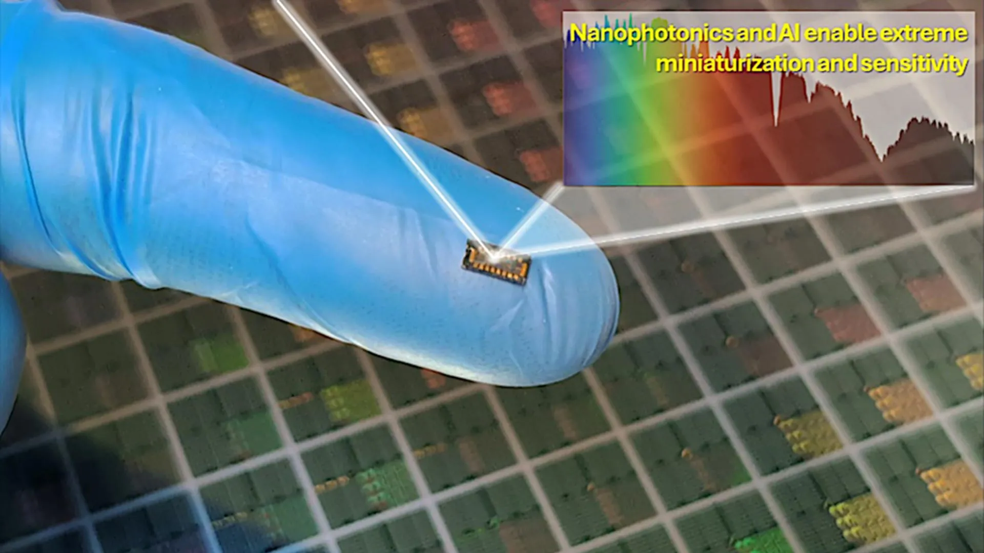
Now, researchers at the University of California, Davis (UC Davis) have developed a dramatically smaller alternative. Writing in progress advanced photonicsthe team describes a spectrometer on a chip so small that it approaches the size of a grain of sand. Rather than relying on large optical components to physically separate light, the new system uses artificial intelligence (AI) and a small array of specially designed sensors to computationally reconstruct the spectrum.
Replace bulky optics with AI
This chip abandons the standard method of spreading light into a rainbow. Instead, it utilizes 16 unique silicon detectors, each designed to respond slightly differently to incoming light. Rather than directly separating individual colors, the detector collects an encoded signal that contains hidden spectral information.
One way to think of this system is as a group of expert tasters sampling different aspects of the same complex mixture. Each detector captures only part of the image. However, when combined, they produce enough information for the AI to reconstruct the original light spectrum.
The second key component is a fully connected neural network trained on thousands of examples. Because the detector signals are noisy and highly encoded, the AI learns the complex relationships between those signals and the actual spectrum of light. This approach solves what researchers call an “inverse problem,” allowing the system to reproduce spectral data with an accuracy of about 8 nm resolution without the use of bulky optical hardware.
Extending silicon into the infrared region
A major advance was made by modifying the surface of a standard silicon photodiode using a special photon-trapping surface texture (PTST). Silicon is typically good for detecting visible light, but has difficulty capturing near-infrared (NIR) light (wavelengths up to 1100 nm). NIR light is particularly important for applications such as biomedical imaging because it can penetrate deeper into human tissues than visible light.
The engineered PTST surface changes the way light behaves within the chip. Rather than NIR photons passing straight through the thin silicon layer, the textured surface scatters the light repeatedly, increasing the likelihood that the silicon will absorb the light. As a result, the chip is more sensitive over a much wider spectral range than standard silicon sensors.
Capturing ultra-fast optical interactions
The new architecture provides functionality beyond simple color detection. The chip also includes a high-speed sensor that can measure the lifetime of a photon with very high temporal precision. This allows the device to detect ultrafast interactions between light and matter that traditional spectrometers may miss completely.
Researchers say this capability could open the door to advanced forms of sensing and imaging that previously required much larger and more expensive systems.
Big potential in a small footprint
The completed system occupies just 0.4 square mm while maintaining high sensitivity and strong immunity to electrical noise, which is a major challenge for portable, low-cost electronics. AI-assisted design helps maintain clear signal quality even in noisy environments.
By combining machine learning and enhanced silicon photodetection, this technology could pave the way for compact real-time hyperspectral sensing devices. Potential applications range from portable medical diagnostics and wearable health monitors to environmental remote sensing and food quality analysis.
