


Detection of light and radiation is essential across the electromagnetic spectrum, but some areas remain particularly challenging. One of these is the terahertz (THz) range, which lies between microwave and infrared radiation. Existing detectors for these frequencies are often slow, lack sensitivity, or rely on large and expensive equipment that frequently requires cryogenic cooling.
Researchers have now developed a compact new detector that combines quantum physics and a specially designed metasurface to significantly improve the way terahertz radiation is captured and converted into electrical signals. Their discovery recently advanced photonics.
A quantum approach to terahertz detection
The new device takes advantage of a phenomenon known as the in-plane photoelectric effect. In this process, incoming terahertz photons transfer energy to electrons trapped within a two-dimensional electron gas. These energized electrons pass through carefully designed potential steps, producing a measurable electrical current.
Unlike traditional photoelectric detectors, this mechanism does not require photons to exceed a minimum energy threshold. Because this process occurs entirely within the plane of the material, it also avoids some of the efficiency limitations that constrained early detector designs.
Previous detectors based on the same principle showed promising sensitivity, but relied on individual antenna elements and could only capture a small fraction of the incoming radiation.
Metasurfaces concentrate radiation into a small detection area
To overcome this limitation, the research team designed the detector around a metasurface, a patterned structure that concentrates electromagnetic energy into a very small area.
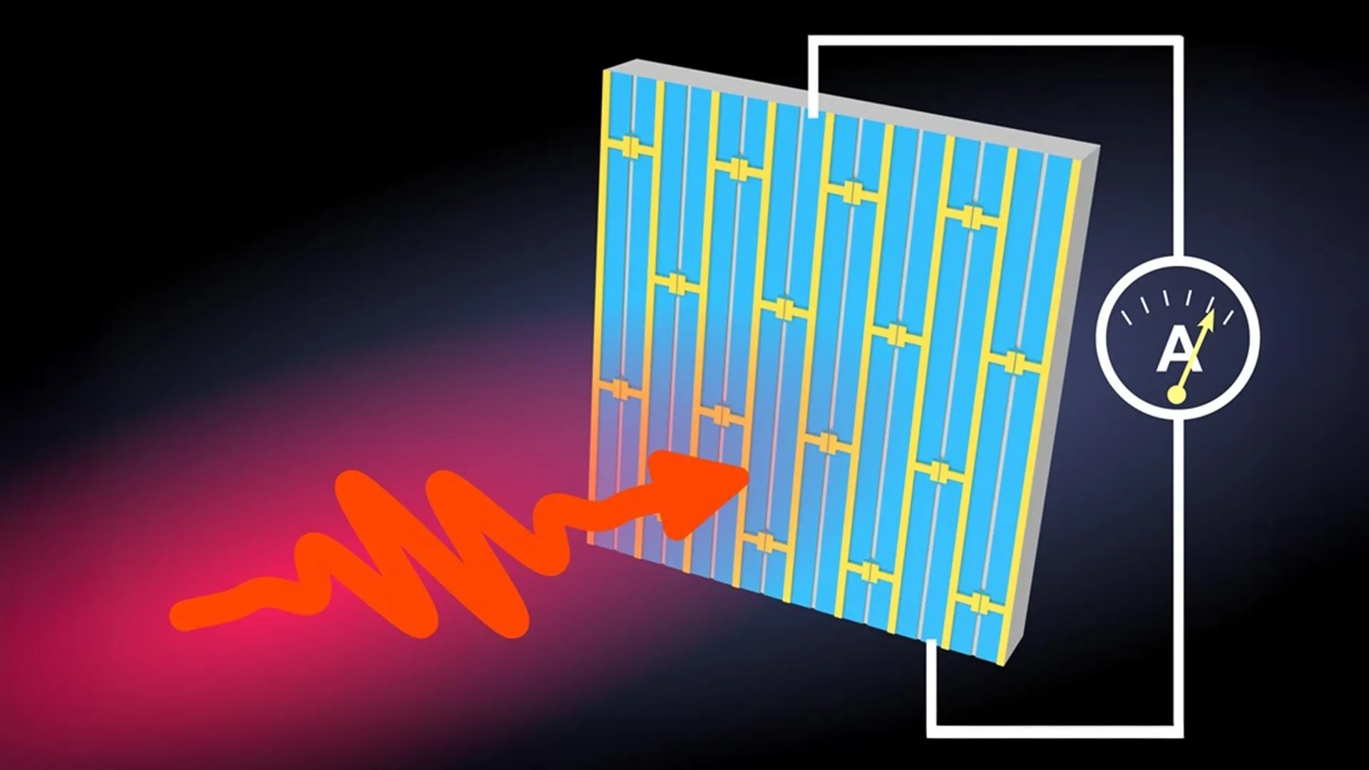
This device uses a repeating “bricklaying” pattern that serves two purposes. It collects the incoming terahertz radiation and directs it into a narrow gap, where the detection process takes place.
Each gap acts as an individual detector. By distributing many of these sensing elements across the surface and linking them electronically, the researchers were able to combine their outputs to produce a stronger overall signal.
This approach eliminates the need for external optics and complex detector arrays. It also ensures that the incident radiation is concentrated only in the areas that directly contribute to signal generation.
Integrating light collection and detection
Rather than designing the detector and light collection system separately, the team started from the metasurface itself and built detection elements directly in regions where the electric field was strongest.
Individual photoelectrically tunable step (PETS) sensing elements are embedded within the capacitive gaps of the metasurface.
“This ensures an optimal coupling between the metasurface and the sensing element,” notes corresponding author Vladisław Michailow, who led the research at the University of Cambridge and then at Swansea University in the UK.
“Compared to the traditional approach of connecting multiple devices in parallel, this approach allowed us to significantly increase detection sensitivity,” adds Michailow.
The researchers used computer simulations to optimize key structural features such as gap dimensions and spacing between repeating units. These parameters determine how tightly the electric field is confined and how much photocurrent is ultimately generated. The final design balances field enhancement and electronic channel width to maximize measurable output.
Semiconductor-friendly design
The detector was fabricated using a semiconductor structure containing a high-mobility electron gas. This manufacturing process is similar to technology already used for field-effect transistors and provides a practical means for integration with existing electronic systems.
The metasurface itself focuses the incident radiation, eliminating the need for external focusing components such as silicon lenses. This could simplify assembly and make large-scale manufacturing more viable.
To test the device, the researchers cooled it to 10 K and exposed it to radiation around 1.9 THz. The detector produced a distinct electrical response that matched the on/off modulation pattern of the input signal.
20x more efficient
Measurements revealed a response of 2.7 Amps/Watt.
This proof-of-concept device also achieved an external quantum efficiency of 2.1 percent at 1.9 THz. This represents an approximately 20-fold improvement compared to previously demonstrated PETS detectors.
According to the researchers, much of this performance improvement is due to the metasurface’s ability to capture a large portion of the incident radiation and focus it directly onto the active region of the detector.
Another advantage is that the detector operates with zero source/drain bias. This eliminates dark current and reduces noise.
“These devices are direct detectors operating at zero bias, so they work without dark current,” said first author Luchao Xia, who fabricated and measured the devices as part of his doctoral research in the Semiconductor Physics Group at the Cavendish Laboratory at the University of Cambridge.
Because the design is geometrically scalable, the same concept could potentially be adapted for use at a wide range of frequencies, from microwaves to mid-infrared wavelengths.
Potential applications across multiple fields
Planar architecture also has practical advantages. Compatibility with standard semiconductor manufacturing techniques allows the detector to be directly integrated into on-chip electronics.
The use of a flat metasurface eliminates the need for precise alignment of external optical components, simplifying packaging and deployment compared to many existing terahertz systems.
The researchers also believe the technology has the potential to operate at higher temperatures than many competing detector platforms. Similar PETS detectors have already demonstrated performance at temperatures that do not require liquid helium cooling and can be achieved with compact cryocoolers.
This will help bridge the critical gap between highly sensitive cryogenic detectors and less sensitive room temperature devices, potentially expanding the range of real-world terahertz applications.
This work represents the first demonstration of a quantum metasurface photodetector based on a two-dimensional electronic system. By combining highly efficient optical capture with highly sensitive quantum detection mechanisms, this work represents an important step towards overcoming long-standing challenges in terahertz technology.
“This result is particularly interesting given the applications that terahertz technology enables in areas such as wireless networks, healthcare, astronomy, biomedicine, and quality assurance in manufacturing,” said co-author David Ritchie, head of the Semiconductor Physics Group.
By integrating metasurface optics directly into the detector itself, researchers are demonstrating how advances in quantum physics and materials engineering can help unlock the full potential of terahertz technology.
